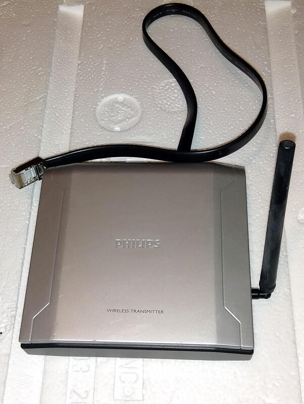
Philips AD906WT Wireless transmitter
Date: 2025-11-17
Overview
This AD906WT/01 wireless transmitter came with a LX3950W/01 home theater system and was paired to an AD906WA/01 receiver1.

Around the mid-2000s, wireless transmitters were offered for home theater systems, as a way to connect the rear speakers without long cables going across a room2.
The wireless transmitter was connected to a specific output on the audio player or amplifier, and it was paired to a matching wireless receiver + amplifier that could power two speakers.

PCB markings are included for SEO, in case someone else might find this while playing with their Philips wireless systems.
Inside view
This looks like analog RF, pre-dating digital protocols. Stickers specifies that the transmitter operates at 864MHz.

There are 2 PCBs, a complex one connected to the antenna, and a simpler one that seems to be here for interconnection with the RJ45 cable.
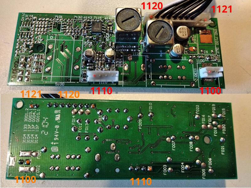
Interface board
This is a 95mm*35mm, dual layer PCB that has 4 JST connectors, and only a few analog components around an dual opamp. Many components are unpopulated.

BOM Identification
| Item | Type | Manufacturer, PN |
|---|---|---|
| 7115 | Dual opamp | JRC 45603 |
| 1100 | Connector | JST, 2-pin |
| 1130 | Connector | JST, 4-pin |
| 1120 | Connector | JST, 8-pin |
| 1121 | Connector | JST, 2-pin |
Connectors pinouts
1100 pinout
- +12V input
- GND
1110 pinout
- ACH1
- AGND1
- ACH2
- AGND2
1120 pinout
- ACH1
- GND
- ACH2
- +12V output
- GND
- GND
- SCL
- SDA
1121 pinout
- SCL
- SDA
Testpoints
| TP | Signal | Connection |
|---|---|---|
| F001 | +12V | 1100.1 |
| F002 | GND | 1100.2 |
| F003 | AGND2 | 1130.4 |
| F004 | ACH2 | 1130.3 |
| F005 | AGND1 | 1130.2 |
| F006 | ACH1 | 1130.1 |
| F007 | ? | Unpopulated |
| F008 | ? | Unpopulated |
| F009 | ACH2 | 7115.7 -> Opamp output |
| F010 | ACH1 | 7115.1 -> Opamp output |
| F011 | ACH1 | 1120.1 -> inductors output |
| F012 | ACH2 | 1120.3 -> inductors output |
| F013 | GND | 1120.2 |
| F014 | +12V | 1120.4 |
| F015 | NC | Unpopulated area |
| F016 | NC | 1130, unpopulated |
| F017 | NC | 1130, unpopulated |
| F018 | NC | Unpopulated area |
| F019 | NC | Unpopulated area |
| F020 | NC | Unpopulated area |
| F021 | NC | Unpopulated area |
| F021 | NC | Unpopulated area |
Board overview
- ACH1: 1130.1 -> filters -> Opamp -> filters -> 1120.1
- ACH2: 1130.3 -> filters -> Opamp -> filters -> 1120.3
All other signals are directly connected from the RJ45 to the 1120 connector. It looks like this board was intended to be used in similar standalone products, looking at the unpopulated components that include footprints for a power jack, a switch and RCA inputs.
There’s an unusual amount of filters, including signal transformers. This rather simple board seems to have been designed with EMC considerations.
PCB markings
Bottom side: - 3104 133 3001.2 - 3104 137 3003.1 - 3104 137 3004.1 - 3104 137 3010.1 - 2104 (datecode) - 1 94V-0 UL (PCB substrate flammability rating)
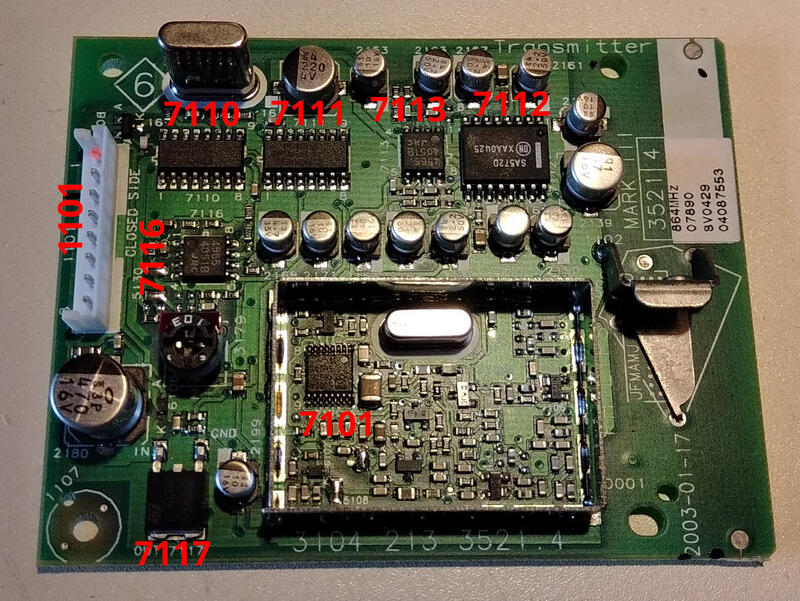
Transmitter board
This is a 80mm*65mm, 4-layer PCB that has one JST connector, one antenna, one RF ASIC in a metal shield, 2 opamps, one analog ASIC, one analog multiplexer and one clock generator.
All components seem to be populated.


BOM Identification
| Item | Type | Manufacturer, PN | |
|---|---|---|---|
| 7101 | I²C-programmable PLL | NXP TSA5060ATS4 | 4MHz crystal |
| 7110 | Oscillator and divider | NXP 74HC4060D5 | 12MHz crystal |
| 7111 | 8-channel analog switch | NXP 74HC4053D6 | |
| 7112 | Audio compressor, AGC | Onsemi SA572D7 | |
| 7113 | Dual opamp | JRC 40658 | |
| 7116 | Dual opamp | JRC 40659 | |
| 7117 | LDO voltage regulator | ST L1117 |
1101 connector pinout
- ACH1
- GND
- ACH2
- +12V input
- GND
- GND
- SCL
- SDA
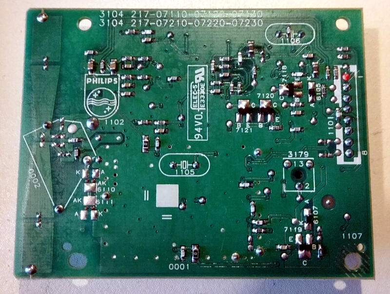
PCB markings
- Sticker:
- 864MHz
- 07890
- SV0429
- 04087553
- Top side:
- PHILIPS
- 2003-01-17
- 3521 4
- Transmitter
- Closed side
- 6
- 3104 213 3521.4
- Bottom side:
- 94V-0 UL (PCB substrate flammability rating)
- ELEC-5
- E3330E
- 3104 217-07110-07120-07130
- 3104 217-07210-07220-07230
- Philips
RJ45 Cable
- ACH2
- AGND
- ACH1
- +12V
- GND
- GND-shield
- SCL
- SDA
Conclusion
This doesn’t seem to be usable without its original equipment or without deeper reverse-engineering, due to the fact the PLL needs I²C data to operate.
References
- ← Previous page
Nuuo NVRmini NV-4080S/Promise NS4600 (3) - Next page →
Philips AD906WA Wireless receiver
Electronics Électronique puissance semiconducteur semiconductors power Hardware CPE INSA Xavier Bourgeois
 RSS - Blog