Philips AD906WA Wireless receiver
Date: 2025-11-18
Overview
This AD906WA/01 wireless receiver came with a LX3950W/01 home theater system and was paired to an AD906WT/01 transmitter1.

Around the mid-2000s, wireless transmitters were offered for home theater systems, as a way to connect the rear speakers without long cables going across a room2.
The wireless transmitter was connected to a specific output on the audio player or amplifier, and it was paired to a matching wireless receiver + amplifier that could power two speakers.

PCB markings are included for SEO, in case someone else might find this while playing with their Philips wireless systems.
Inside view

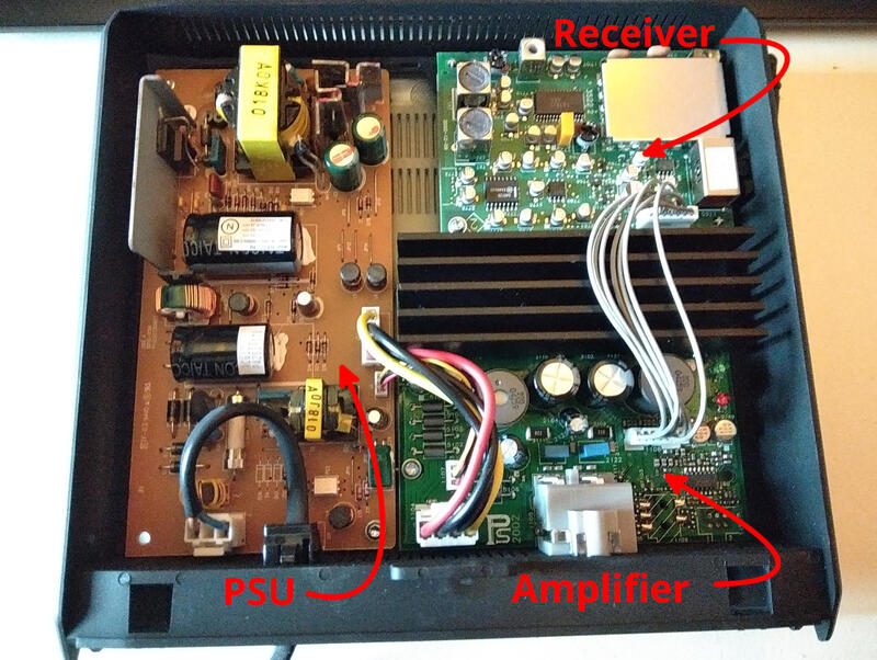
There are 3 PCBs :
- Switching PSU
- Power amplifier
- RF receiver
PSU
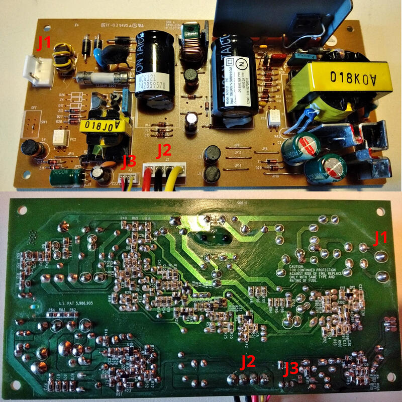
This is a 150mm*75mm, single-layer PCB. It looks like there are 2 flyback supplies, one with a small transformer, likely for a low-power output, and one with a larger transformer and two outputs, likely for the power amplifier.
Interestingly, there’s no monolithic IC. The control-side only has semiconductors in SOT-23 package.

Specifications
The sticker specifies the following data:
- Model: AC6121
- Input 100~240V 50-60Hz 0.34A
- Output:
- +29.5V/0.16A
- -29.5V/0.16A
- 10V/0.2A
Connectors
There are 3 connectors on the PCB:
- J1: AC input, unearthed
- J2: Power output
- J3: Standby output
J2 pinout
| Pin | Wire color | Signal |
|---|---|---|
| J2.1 | Yellow | -29.5V |
| J2.2 | Black | GND |
| J2.3 | Black | GND |
| J2.4 | Red | +29.5V |
J3 pinout
| Pin | Wire color | Signal |
|---|---|---|
| J3.1 | Yellow | PG? |
| J3.2 | Black | GND |
| J3.3 | Red | 10.0V |
The signal on the pin 1 seems to act as a power good signal. This would need to be confirmed.
PCB markings
- Sticker:
- AC6121
- P42859578
- Top side:
- TF-03
- 94V0 UL
- SIDE A
- 855D-016K
- PI ELECTRONICS
- Bottom side:
- SIDEB
- U.S. PAT 5,986,905
Amplifier
This is a 100mm*90mm, dual-layer PCB with a heatsink.

Connectors
1100 pinout
- Power output L
- GND
- GND
- Power output R
1104 pinout
Warning the markings are reversed compared to the PSU.
- +29.5V
- GND
- GND
- -29.5V
1106 pinout
- Audio input R
- GND
- Audio input L
- 10V output
- GND
- ?
- Red LED input
1107 pinout
- 10V input
- GND
- PG input?
BOM identification
| Item | Type | Manufacturer, PN |
|---|---|---|
| 7100 | Quad opamp | Natsemi LM8373 |
| 7101 | Dual power amplifier | Philips TDA8920TH4 |
LEDs
- 6109: Green, Power-on
- 6110: Red, receiver paired
PCB markings
- Top side:
- PS 2002
- 94V-0 UL (PCB substrate flammability rating)
- 2004 (datecode)
- Bottom side:
- 3104 123 4365. 2
Receiver Board
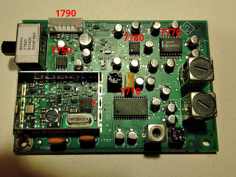
This is a 90mm*68mm, 4-layer PCB that has one JST connector, one antenna, one RF ASIC in a metal shield, one opamps, one MCU, two analog ASICs, and one unknown chip.


1790 connector pinout
- Audio output R
- GND
- Audio output L
- 10V input
- GND
- ? (3V when powered-on)
- Red LED output
BOM identification
| Item | Type | Manufacturer, PN | |
|---|---|---|---|
| 7710 | PLL, IF demuxer | Sanyo LA18365 | |
| 7750 | 8-bit MCU | PIC12C5086 | |
| ? | I²C-programmable PLL | NXP TSA5060ATS7 | 4MHz crystal |
| 7770 | Audio decompressor, AGC | Onsemi SA572D8 | |
| 7780 | Dual opamp | JRC 40659 | |
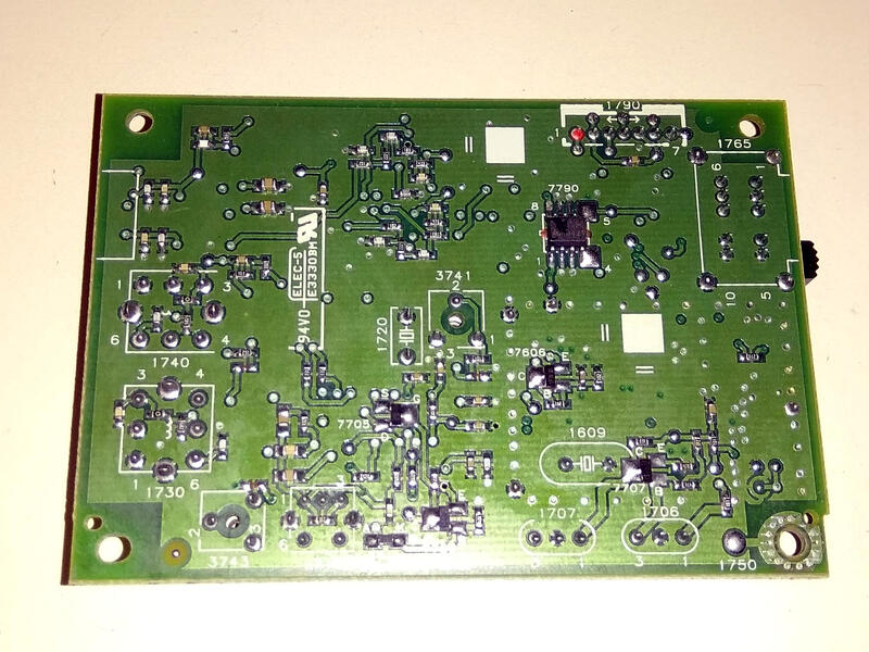
| 7790 | Unreadable | ST ??C80 |
PCB markings
- Sticker:
- 864MHz
- 07520
- SV0430
- 04091554
- Top side:
- 3522 2
- 2002-12-09
- 2
- Bottom side:
- 94V-0 UL, PCB substrate flammability rating
- ELEC-5
- E3330BM
Usability
The transmitter isn’t designed to operate without its Philips LX3950W/0110, which I don’t have, so using the receiver as intended looks compromised.
However, the amplifier works without the RF part, by connecting analog audio signals on the connector 1106: L-R signals on pins 1 and 3, and GND on pin 2.
Funnily, the specsheet gives the “Output power (RMS): 5 x 45 W”11 and the amplifier’s datasheed specifies a maximum power of 70W for each channel, when the receiver can only draw 25W from the power outlet and its PSU delivers 9.44W on its +/- 29.5V rails. That looks questionable.
This is a Class D amplifier, which explains why there’s a low-pass filter on the output, and why the heatsink is rather small for the advertised power.
References
- ← Previous page
Philips AD906WT Wireless transmitter - Next page →
cms
Electronics Électronique puissance semiconducteur semiconductors power Hardware CPE INSA Xavier Bourgeois
 RSS - Blog